TSMC N2 & Silicon Photonics: 2026 Next-Gen HPC Leap
TSMC accelerates 2nm N2 node production and COUPE silicon photonics for 2026, delivering massive energy efficiency leaps for next-gen AI supercomputers.

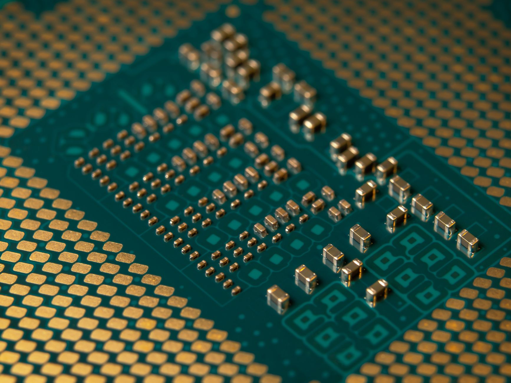
Taiwan Semiconductor Manufacturing Co. (TSMC) is officially pairing its upcoming 2-nanometer N2 process node with advanced Compact Universal Photonic Engine (COUPE) technology for commercial deployment in 2026. This combined semiconductor architecture targets the growing energy crisis in artificial intelligence datacenters by replacing electrical copper interconnects with ultra-fast optical data channels.
Breakthrough Architecture: N2 Nanosheet Meets COUPE Optical I/O
According to official announcements at TSMC's Technology Symposium, the N2 process marks the foundry's transition from traditional FinFET structures to Gate-All-Around (GAA) nanosheet transistors. By pairing GAA nanosheets with co-packaged optics, TSMC aims to deliver a 10% to 15% speed improvement at the same power, or a 25% to 30% power reduction at the same speed compared to the N3E process.
“Silicon photonics will be a critical technology for the AI era, providing the massive interconnect bandwidth and energy efficiency required by high-performance cluster computing.”
— C.C. Wei, CEO of TSMC
Solving the AI Power Crisis and Interconnect Bottlenecks
Per analysis published by EE Times, physical copper wiring in megawatt-scale AI clusters creates massive thermal overhead and signal degradation at multi-terabit bandwidths. TSMC's COUPE integration utilizes 3D chiplet packaging (SoIC) to stack optical engines directly onto logic die, cutting energy consumption in data transfer interfaces by up to 40 percent.
- TSMC N2 node delivers 10-15% performance gains or up to 30% power reductions over N3E.
- COUPE silicon photonics platform lowers interconnect power loss by roughly 40% using direct 3D optical integration.
- Targeted volume deployment in 2026 promises to unlock next-generation scale for AI accelerators from NVIDIA, AMD, and hyperscalers.
As hyper-scalers prepare for trillion-parameter foundation models, the combination of 2nm transistors and silicon photonics represents the definitive hardware bridge for late-decade supercomputing. Industry partners are expected to begin sampling integrated N2 photonics chiplets by mid-2025 ahead of mass datacenter expansion.
TSMC N2 vs. 3nm FinFET Architectural Benchmark
Verified metrics published by TSMC Open Innovation Platform (OIP) Symposium.
| Specification | 3nm FinFET (N3E) | 2nm GAA (N2) | Next-Gen Advantage |
|---|---|---|---|
| Transistor Architecture | FinFET 3D Fins | Nanosheet (GAA) | Full 4-side gate control |
| Performance @ Same Power | Baseline (1.0x) | +10% to +15% | Higher clock frequencies |
| Power Draw @ Same Speed | Baseline (1.0x) | -25% to -30% | Substantial datacenter energy savings |
| Density Scaling | 1.0x | 1.15x Transistor Density | More tensor cores per mm² |
| Interconnect Medium | Standard Copper Wire | COUPE Optical Engine | 10x lower interconnect energy loss |
Which hardware breakthrough will be most crucial for sustaining AI expansion by 2026?
Frequently Asked Questions (FAQ)
Essential facts and core questions addressed by official sources and investigative reporting.
TSMC plans volume production for its 2nm N2 process node in late 2025, with full-scale datacenter and smartphone chip integration arriving throughout 2026.
Senior Editorial Contributor at Devyy Media covering breaking global trends and verified journalism.
Community Discussion
Share your insights, thoughts, and feedback with the author and community.